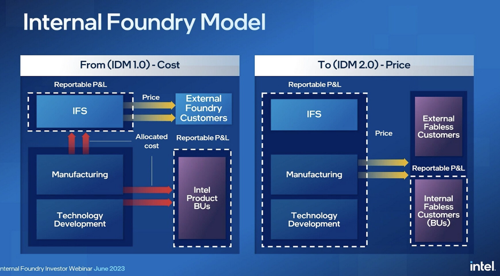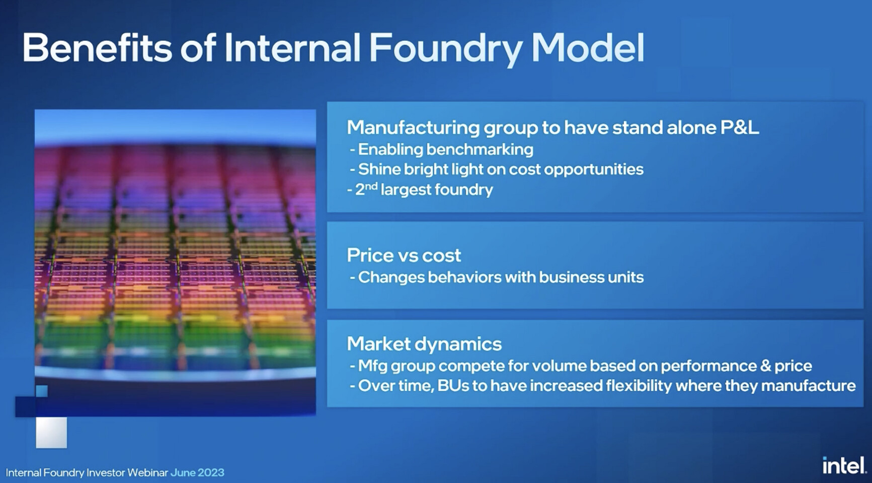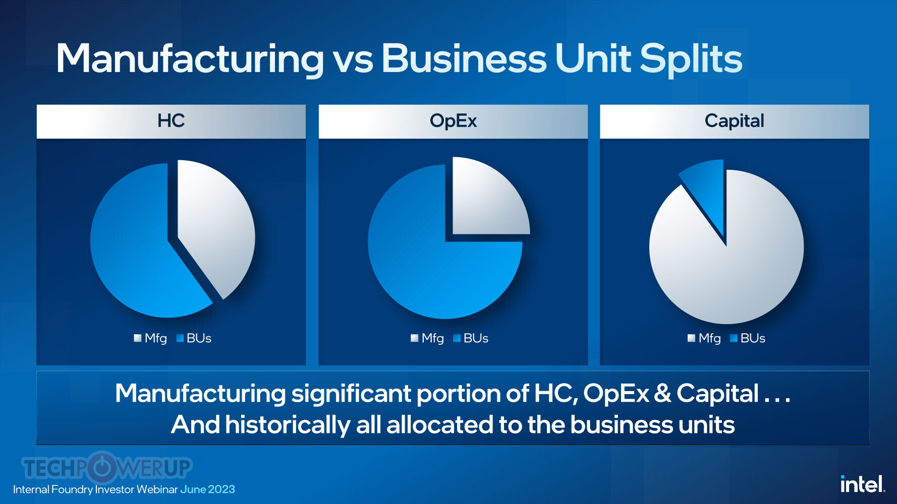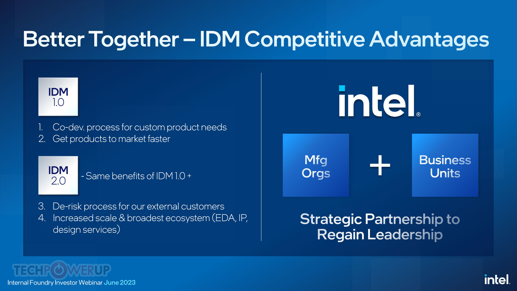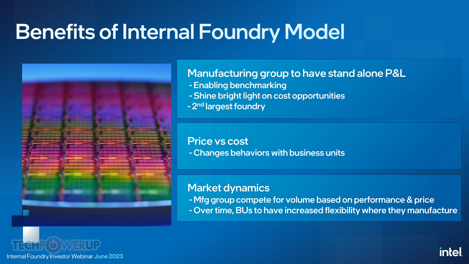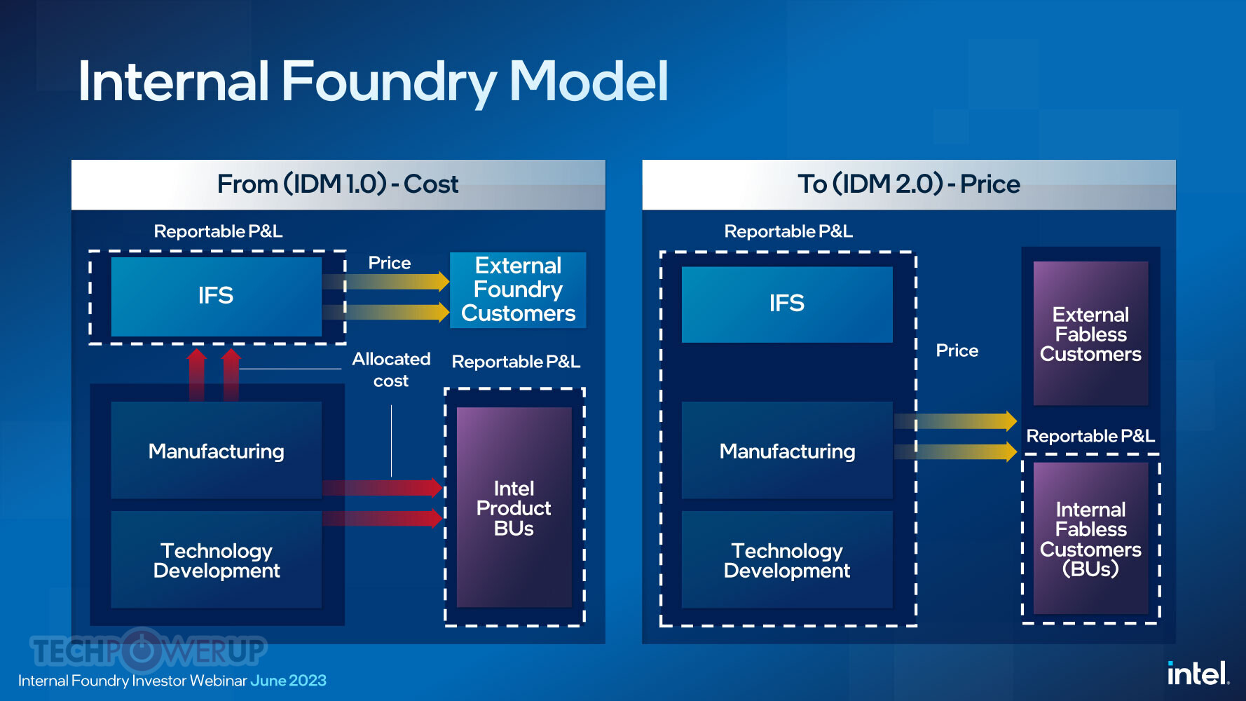
Intel has been facing challenges with its integrated device manufacturing (IDM) in recent years, and it is no longer a leading-edge semiconductor manufacturer, with TSMC taking the top spot. However, the company hopes to increase its efficiency and establish itself as the go-to foundry for customers through a new restructuring plan. David Zinsner, Executive Vice President and Chief Financial Officer, and Jason Grebe, Corporate Vice President & GM of the Corporate Planning Group at Intel, explained to investors how IDM will transform into a next-generation business. Intel IDM, including Intel Foundry Services (IFS), will adopt a new operational model, which will make IDM an almost separate business unit with its own profit and loss (P&L) statement published in the quarterly/yearly financial report.
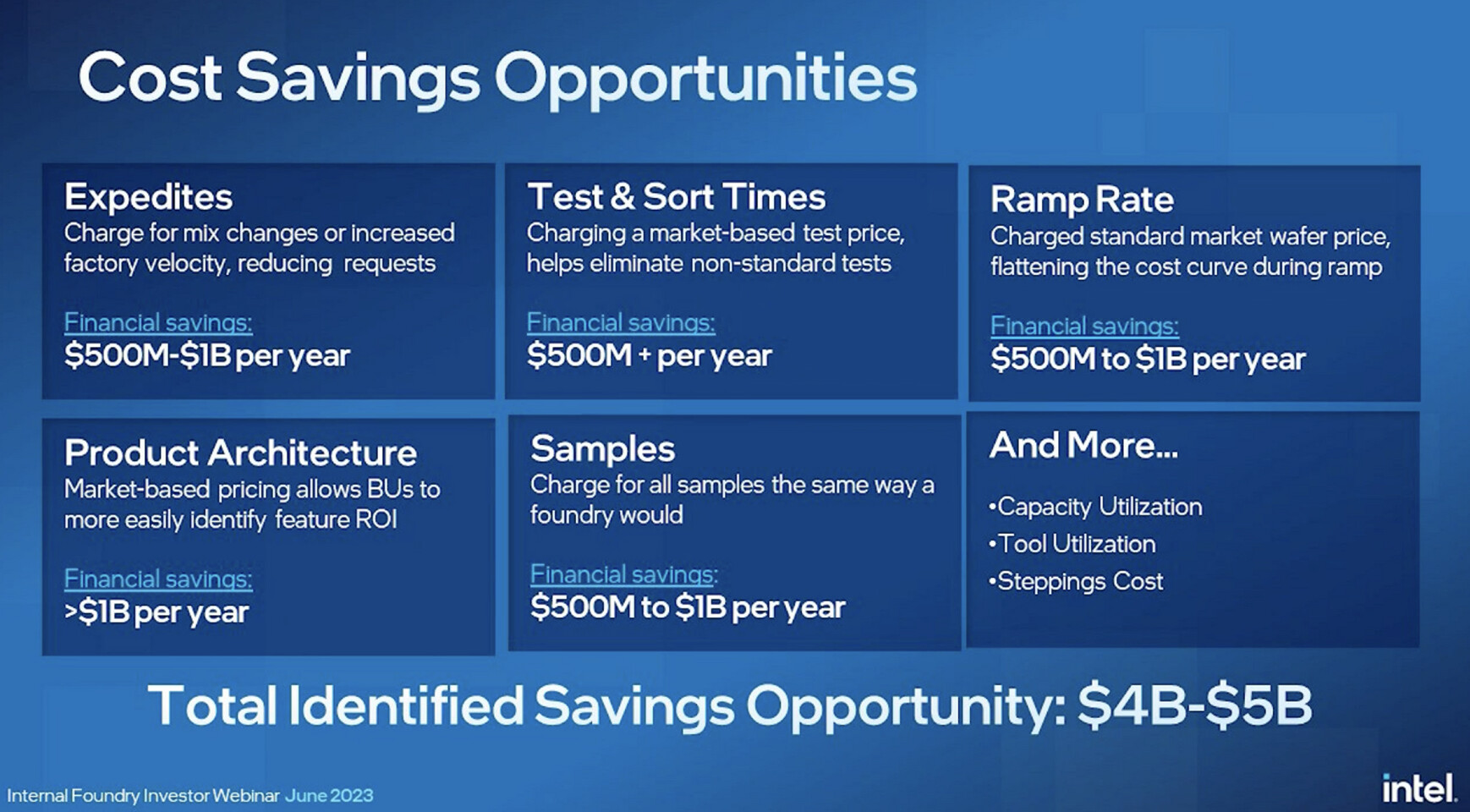
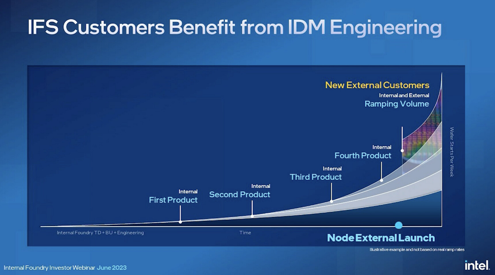
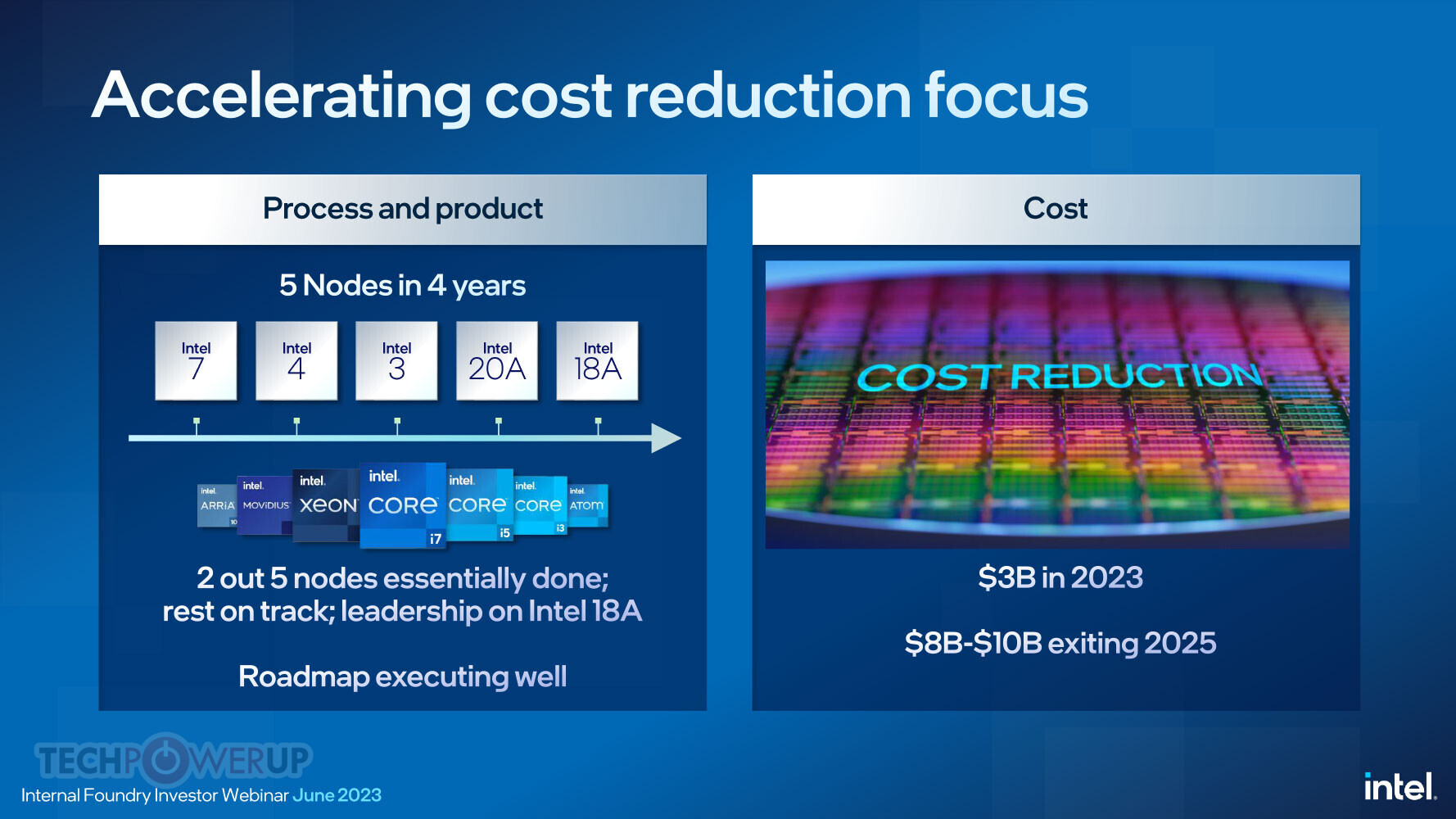
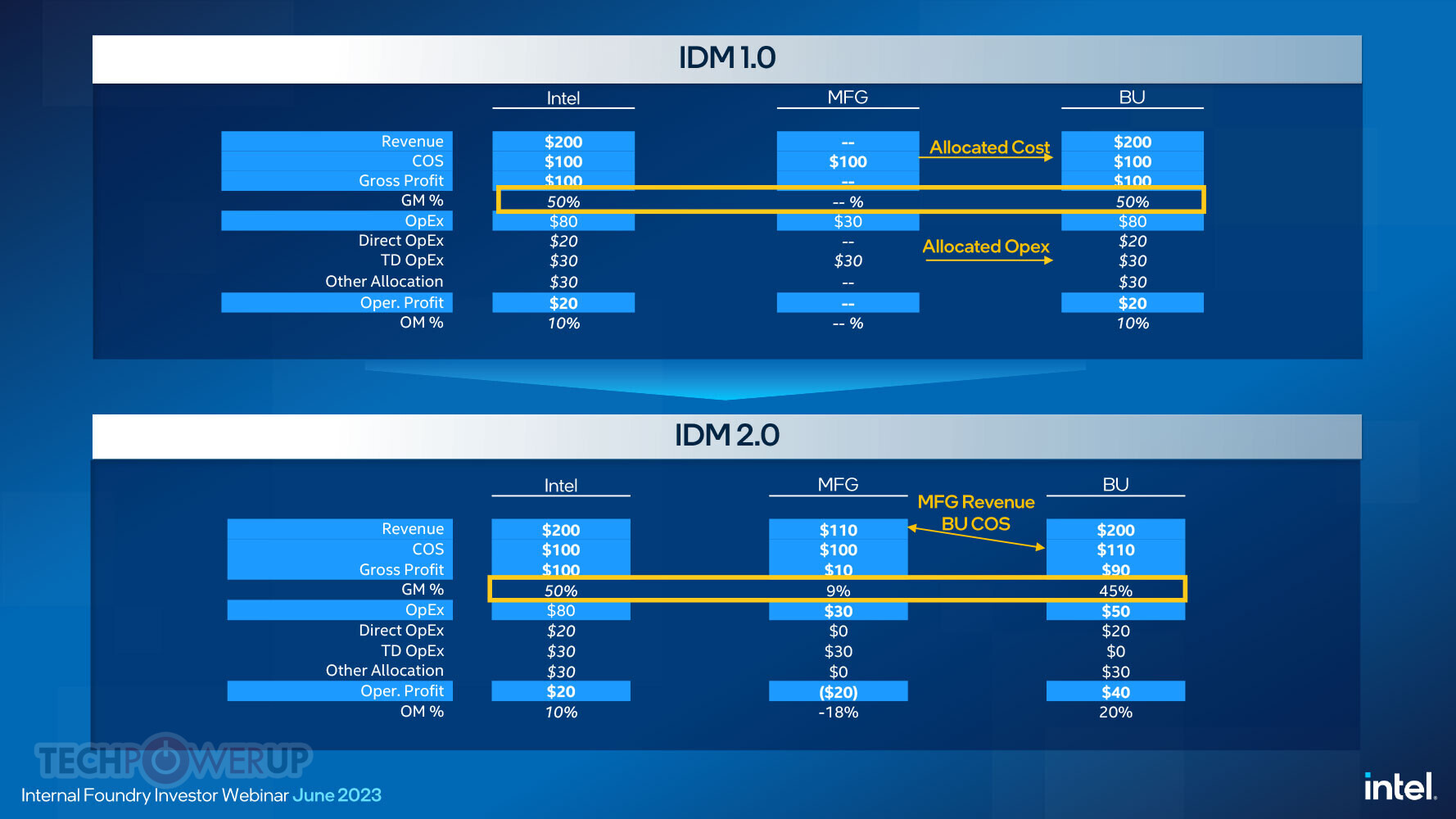
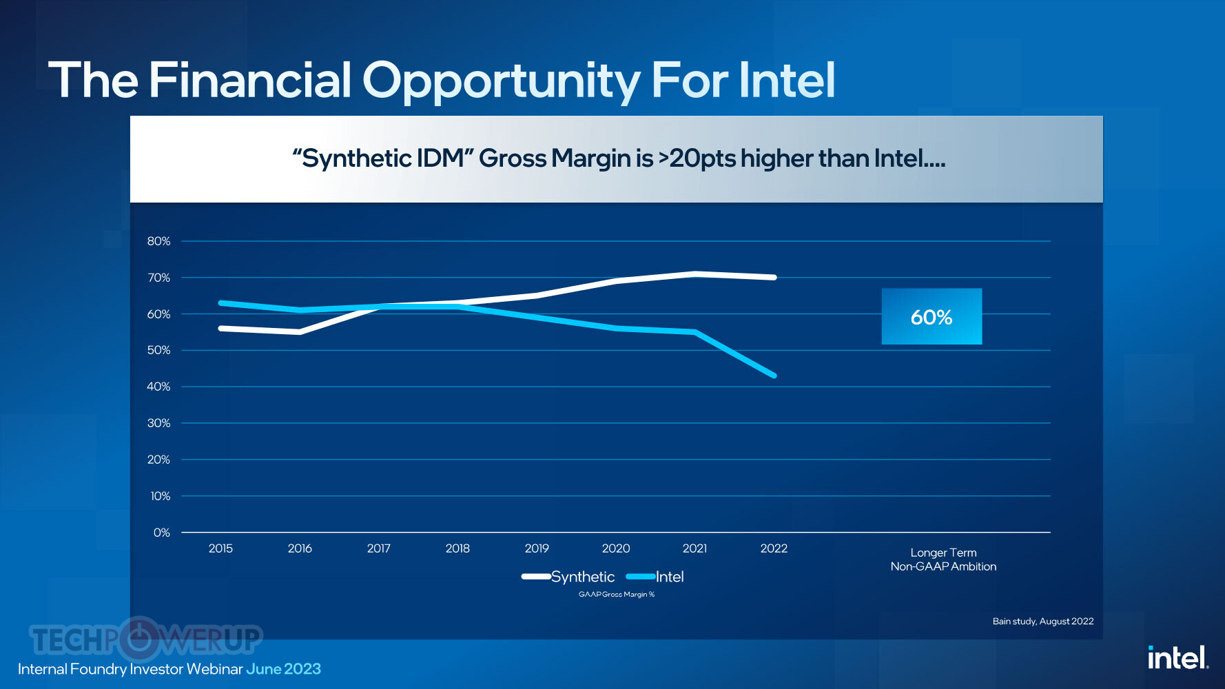
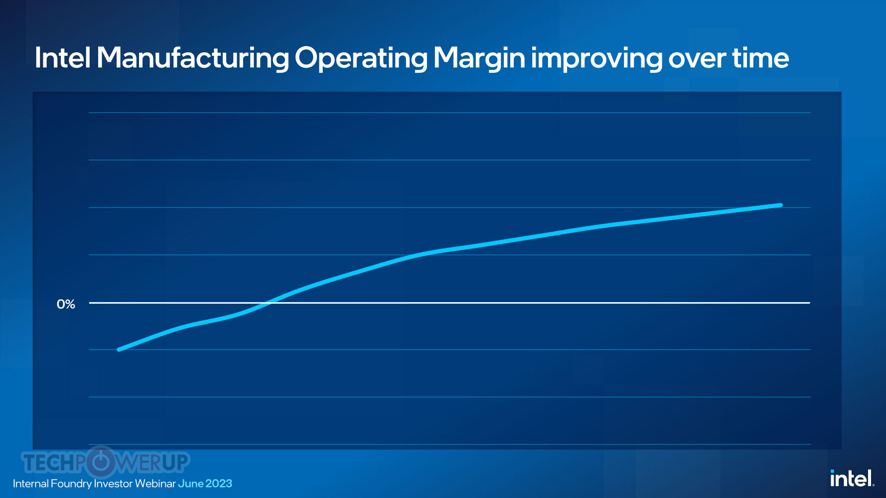
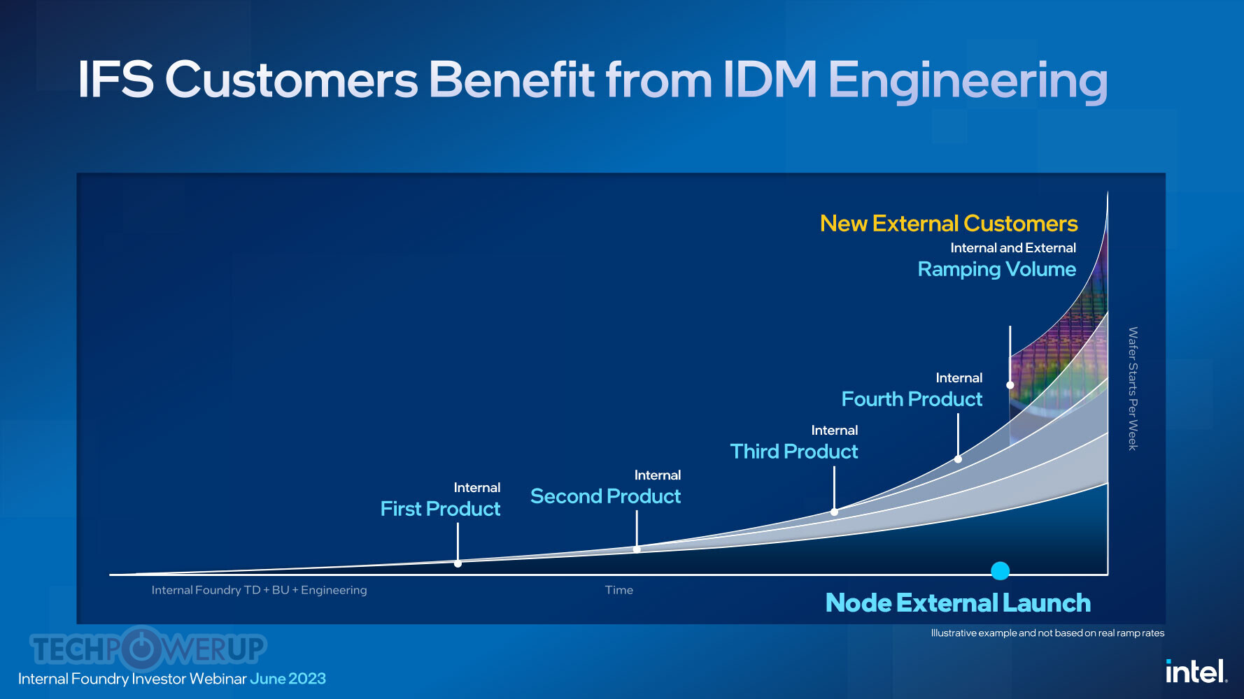
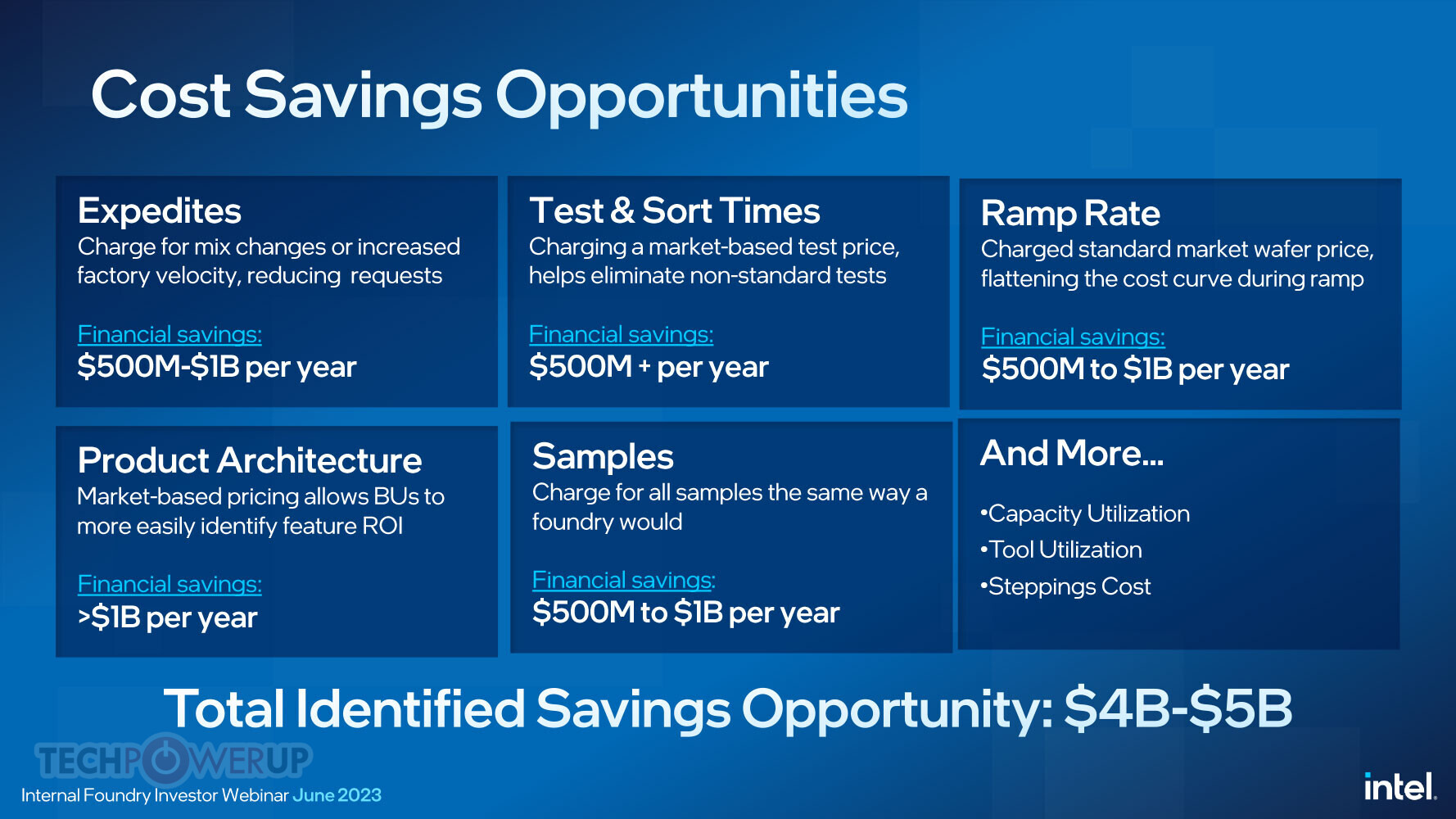
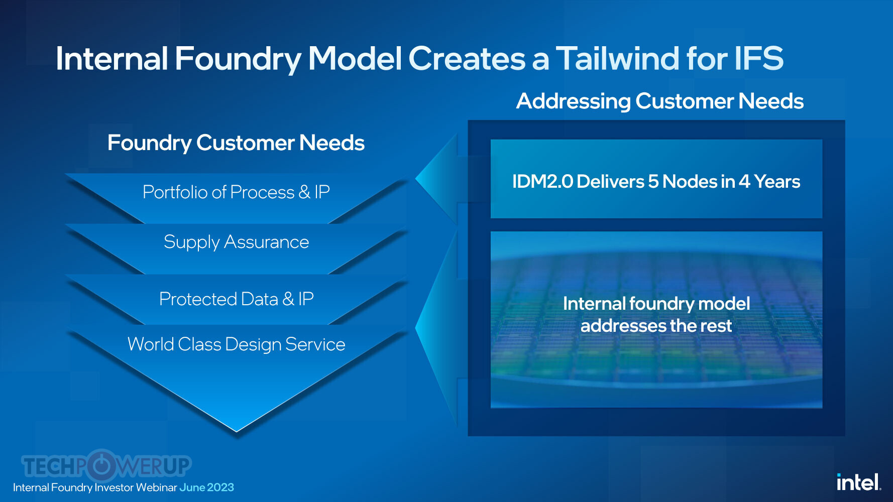
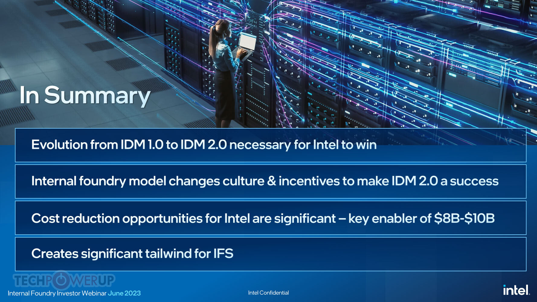
According to Intel, the company's IDM 1.0 strategy has been successful, but IDM 2.0 is needed to build next-generation nodes as the capital required for them is massive. Intel hopes to regain node leadership with the Intel 18A node in 2025. The company's strategy is still to have IFS as the second biggest external foundry business, presumably just behind TSMC. Putting IDM into its own P&L will result in $8-10 billion in "cost reduction opportunities," including ramp rates, test time, and sort times based on market pricing, not Intel's pricing. At the start, IDM is expected to have a negative operating margin. Intel also states that keeping IFS as a business unit allows the company to simultaneously develop products on it and de-risk it for customers who want to build on IFS. The company is developing five different products (assuming packaging) on Intel 18A, all of which will be available for customers to use as well. Jason Grebe stressed that there will be complete segregation of customer data and IP, with world-class service and support, so upcoming customers can trust the company. David Zinsner was asked why Intel didn't just split into a fabless design business and a separate foundry business. He noted that they thought there is a lot of benefit of combining design and manufacturing business, especially as having Intel as customer zero, which can translate its knowledge of working with new technologies to other customers.
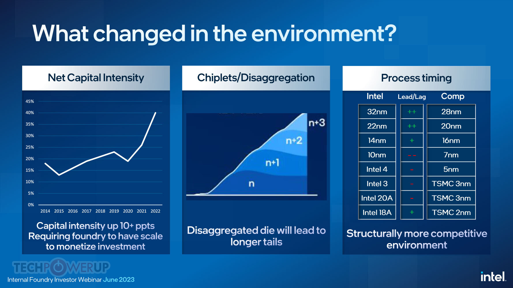
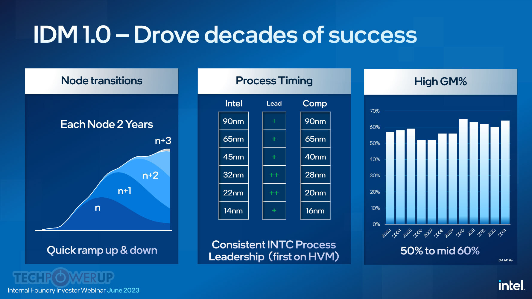
A pair of slides in the slide deck below compare Intel's foundry node advancement to those of its competitors. It details how Intel maintained a technological and first-to-market lead over TSMC across their 90 nm-class, 65 nm-class, 45 nm-class, 32 nm-class, 22 nm-class, and 14 nm-class. The company's 10 nm node was significantly delayed, which gave TSMC 7 nm free reign over the next-generation market for over a year. Intel marks 10 nm (aka Intel 7) as significantly lagging behind TSMC 7 nm on time-to-market. TSMC 5 nm has already been in the market for over 3 quarters now, and it's only later in Q3 that Intel could release the first products based on the rival Intel 4 node ("Meteor Lake" compute tile). Intel 3 could similarly lag by a couple of quarters behind TSMC 3 nm, as could Intel 20A. It's at the 2 nm-class where Intel claims that if it executes the IFS and IDM 2.0 roadmap correctly, the Intel 18A foundry node should beat TSMC 2 nm-class nodes both technologically and on time-to-market.
The complete slide deck follows.