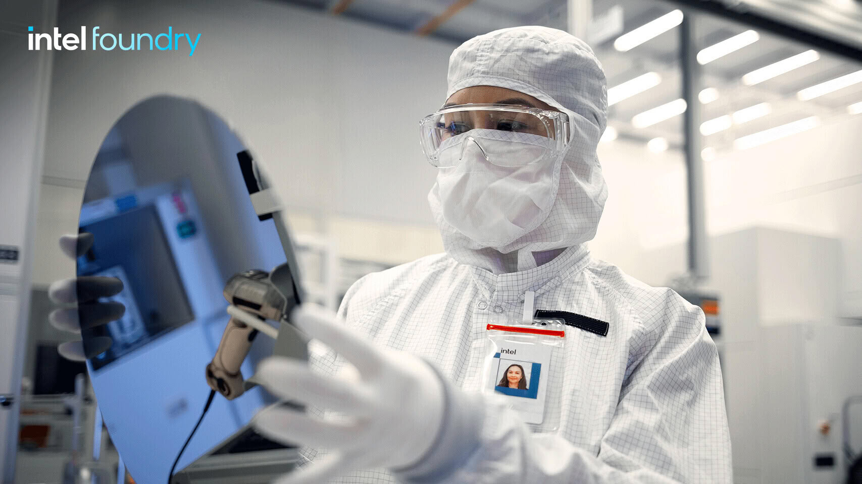
Intel Achieves Strong Q2 2026 Growth and Accelerates 14A Node Production Timeline
Intel has announced impressive financial results for the second quarter of 2026, reporting revenue of $16.1 billion and robust cash flow. Beyond the strong financials, a significant focus of the company’s recent earnings call was the progress and updated schedule for its advanced 14A process node.
14A Node Production Moves Ahead of Schedule
During the earnings call, Intel CEO Lip-Bu Tan highlighted the company’s accelerated roadmap for the 14A node. “With encouraging progress from external customers and increased demand for our internal products, we remain on track for 14A risk production for our internal products in the second half of 2027. We decided in Q2 to fully commit to a high-volume ramp in 2028,” Tan stated. This revised timeline brings high-volume manufacturing forward by a full year compared to previous projections, strengthening Intel’s position in delivering cutting-edge semiconductor technology for both its own products and external foundry customers.
Defect Rate Improvements and Yield Optimization
Recent data indicates that Intel’s 14A node currently achieves a defect density (D0) of 0.5, meaning that defects occur at a rate of 0.5 per unit area during production. This low defect rate is a positive indicator for manufacturing efficiency, as it translates to a limited amount of non-functional silicon. For example, the “Panther Lake” compute tile, with a die size of 114.304 mm², currently yields approximately 56.45% at this defect rate.
Intel is actively working to further reduce the defect rate to D0=0.1, a target that would enable yields of 80-90%. Achieving this milestone is expected by the time high-volume production begins in 2028, significantly improving manufacturing output and cost efficiency.
Process Design Kit (PDK) Milestones and Customer Enablement
Intel has also completed version 0.5 of its process design kit (PDK) for the 14A node, a critical toolset for chip designers. The company plans to release version 0.9 of the PDK to customers in October, providing a production-like environment for trial runs in the second half of 2027. This step is essential for customers to validate their designs and prepare for volume manufacturing in 2028.
Increased Investment in Foundry Capabilities
To support these advancements, Intel is raising its capital expenditure for the year to over $20 billion. The majority of this investment will be directed toward upgrading Intel Foundry operations and modernizing facilities, ensuring the company remains at the forefront of semiconductor manufacturing technology.
Intel’s accelerated 14A node timeline, ongoing yield improvements, and substantial investments underscore its commitment to innovation and leadership in the semiconductor industry.